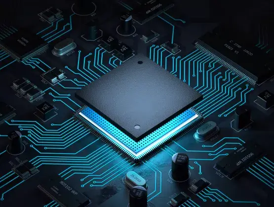
The relentless pursuit of faster and more energy-efficient electronics has driven innovation in chip design, and MIT researchers are at the forefront of this revolution. They have unveiled an innovative 3D chip design that promises to significantly improve the performance and energy efficiency of future technologies. This breakthrough could have a profound impact on various sectors, ranging from mobile communications to artificial intelligence and quantum computing.
For years, the electronics industry has faced limitations in packing more transistors onto traditional 2D chips. As the industry approaches the physical limits of miniaturization, manufacturers are exploring new ways to enhance chip performance. MIT engineers have responded by developing a method to stack multiple layers of transistors and semiconducting elements, effectively transforming the traditional "ranch house" chip into a "high-rise."
The key to MIT's innovation lies in a novel fabrication process that integrates high-performance Gallium Nitride (GaN) transistors onto standard silicon CMOS chips. GaN is a semiconductor material known for its superior speed and power efficiency compared to silicon. However, its high cost and the specialized processes required to incorporate it into conventional electronics have limited its widespread adoption.
MIT researchers have overcome these challenges by developing a low-cost, scalable technique compatible with existing semiconductor foundries. Their method involves building tiny transistors on a GaN chip, cutting out individual transistors, and bonding only the necessary number onto a silicon chip using a low-temperature process. This approach minimizes the amount of GaN needed, significantly reducing costs while still delivering a substantial performance boost from the compact, high-speed transistors.
Furthermore, by separating the GaN circuit into discrete transistors spread across the silicon chip, the technology effectively reduces the overall system temperature. This thermal management is crucial for maintaining optimal operating conditions and enhancing the reliability of electronic systems. In essence, the new design combines the strengths of silicon and GaN, creating hybrid chips with the potential to revolutionize commercial markets.
The implications of this technology are far-reaching. For example, the researchers have used this process to create a power amplifier, a critical component in mobile phones. This amplifier achieves higher signal strength and efficiency than traditional silicon transistor-based devices. In smartphones, this could lead to improved call quality, faster wireless bandwidth, enhanced connectivity, and extended battery life.
Beyond mobile devices, MIT's 3D chip design could revolutionize other fields. Its ability to pack more transistors into a smaller space while reducing energy consumption makes it ideal for artificial intelligence, telecommunications, and medical devices. The development of advanced AI algorithms, faster wireless communication networks, and more sophisticated medical imaging equipment could all benefit from this technology. The chips also show promise for quantum computing, as GaN performs better than silicon at cryogenic temperatures.
Looking ahead, MIT researchers are focused on further scaling and industrializing their 3D chip technology. They envision that this method could be used to build AI hardware in stacked chips for laptops or wearable devices, rivaling the speed and power of today's supercomputers while offering vast data storage capabilities. A spinout company has even been formed to bring this technology to market, aiming to revolutionize the semiconductor industry with more efficient AI hardware and compact electronics.
In conclusion, MIT's innovative 3D chip design represents a significant leap forward in semiconductor technology. By integrating high-performance GaN transistors onto standard silicon chips in a cost-effective and scalable manner, this technology promises to unlock new levels of speed, energy efficiency, and performance in future electronics. From mobile devices to AI hardware and beyond, the potential applications of this breakthrough are vast and transformative. As researchers continue to refine and commercialize this technology, we can expect to see a profound impact on the electronics landscape, ushering in an era of smarter, faster, and more efficient devices.